On 19th January 2017, I started the process of making a printed circuit board for my 23cm amplifier project. I was extremely pleased with the results so thought I would write an article and make a video that shows how I did it.
If you would like to take a look at my 23cm liquid cooled amplifier project click here.
PARTS / EQUIPMENT LIST
Below are the parts / equipment I used in this project. I have include ‘Buy’ links that link to products available to purchase on Amazon.
- G6ALU PCB PDF – download from Radio-Kits website
- Press-n-Peel transfer film
- PCB (Printed Circuit Board)
- Household iron
- Rubber gloves
- Sharpie fine point permanent marker pen
- Newspaper
- Glass dish i.e. Pyrex
- A4 sheet of paper
- Fibreglass single sided PCB board
- Ferric chloride etching solution
- Steel wool
- PCB and flux cleaner
- Goggles
MY ‘HOW TO MAKE A PCB AT HOME’ VIDEO
This video contains all of the steps contained in this article.
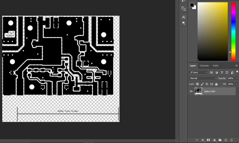
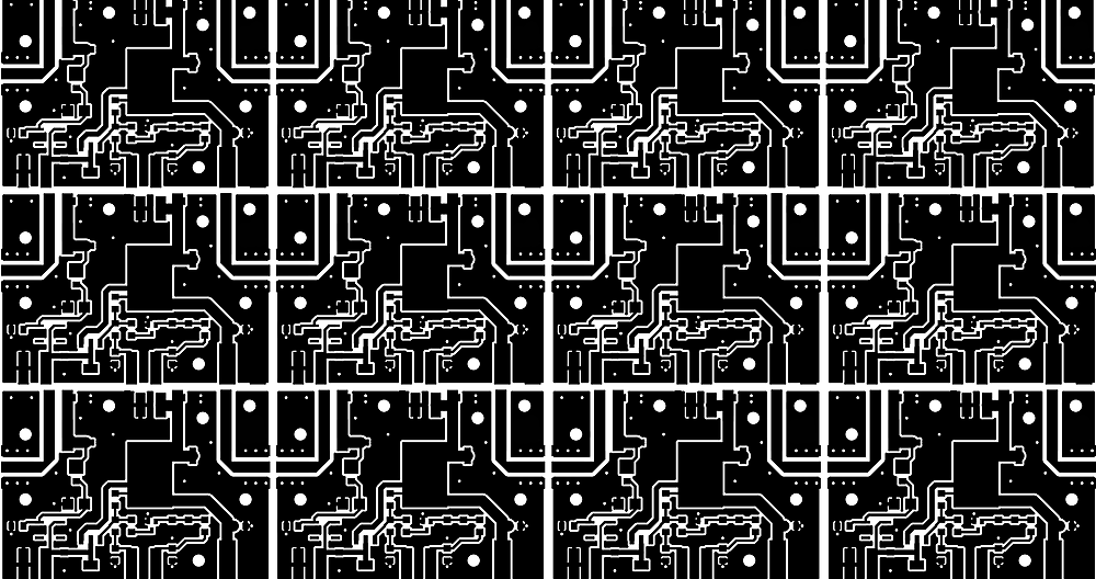
PCB SCHEMATIC
I downloaded the PCB schematic in PDF format from the Radio-Kits website. The PCB was not to scale and contained some blurriness around the tracks.
Using Photoshop CC 2017 I created a canvas the size of the transfer film (216mm x 279mm), cleaned up the tracks and made some minor changes to track layout. I then scaled the image.
Remember the image must be reversed.
PRINTING TO TRANSFER FILM
The transfer film I purchased is for laser printers and will not work with inkjet. I used a commercial grade printer set to highest quality settings. The transfer film has a glossy surface and a matt surface. The matt side is the side you must print on.
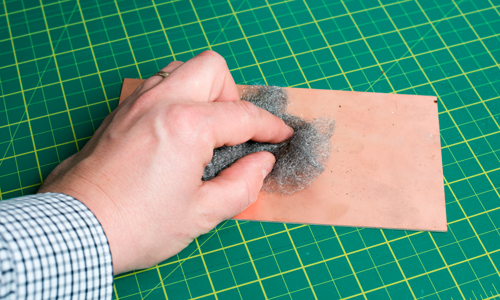
REMOVE PROTECTIVE COATING FROM PCB
Using steel wool I removed all of the protective film from the surface of the PCB. Once all of the film was removed I moved the wire wool along the length of the PCB in horizontal lines to key the copper in one direction.
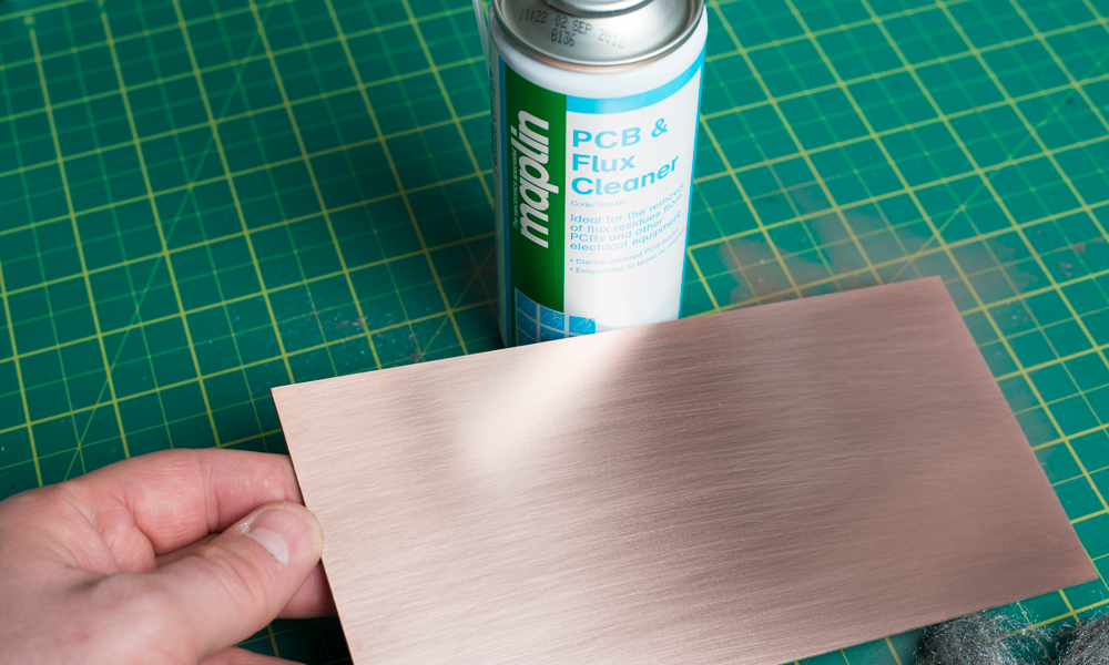
INSPECTION AND CLEANING PCB
I inspected the board to ensure all of the film was removed and then cleaned it with PCB and flux cleaner. You can see in the photo that it is now shiny and keyed in one direction.
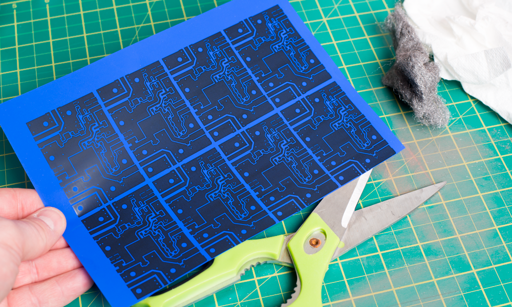
FILM PREPARATION
Using scissors I cut a strip of three boards from the film.
TRANSFER PCB SCHEMATIC FROM BOARD TO PCB
I placed a newspaper on my work surface and placed the PCB copper side up. I then laid the film on top of the PCB print side down (matt side) and carefully laid a sheet of A4 paper on top of the film ensuring no movement.
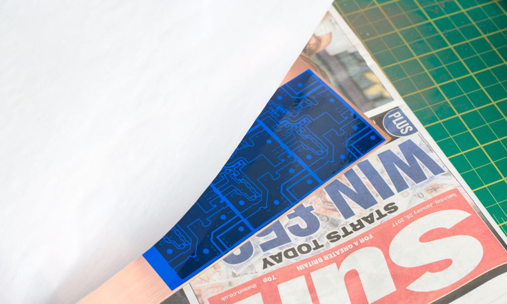
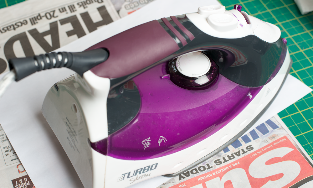
I placed my wife’s iron (she was out) on top of the paper ensuring all of the film was covered and left it for around two minutes.
The manufacturers of the film recommend setting the iron to a temperature between 200°C and 250°C with steam switched off. My iron doesn’t have temperature indicators so I put it on highest temperature setting. You may need to experiment to see which settings work best for you.
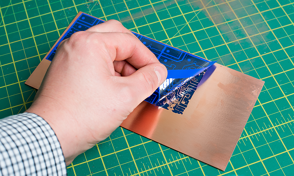
REMOVING THE FILM
I left the PCB to cool a couple of minutes before quenching in cold water. After drying the board I then left it for a few more minutes until fully cool.

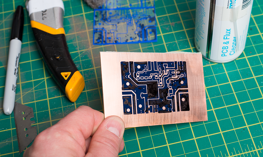
Starting at one corner I slowly peeled off the film.
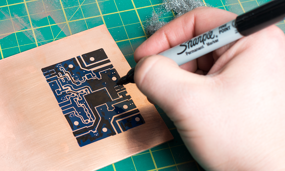
TOUCHING UP
Most of the film adhered to the PCB very well but there were a few places where it didn’t. I used a black ‘Sharpie’ permanent marker to touch up. Permanent marker ink is not affected by the etching solution.
Using a Stanley knife I cut out one of the boards by scoring it several times and snapping it.
ETCHING THE PCB
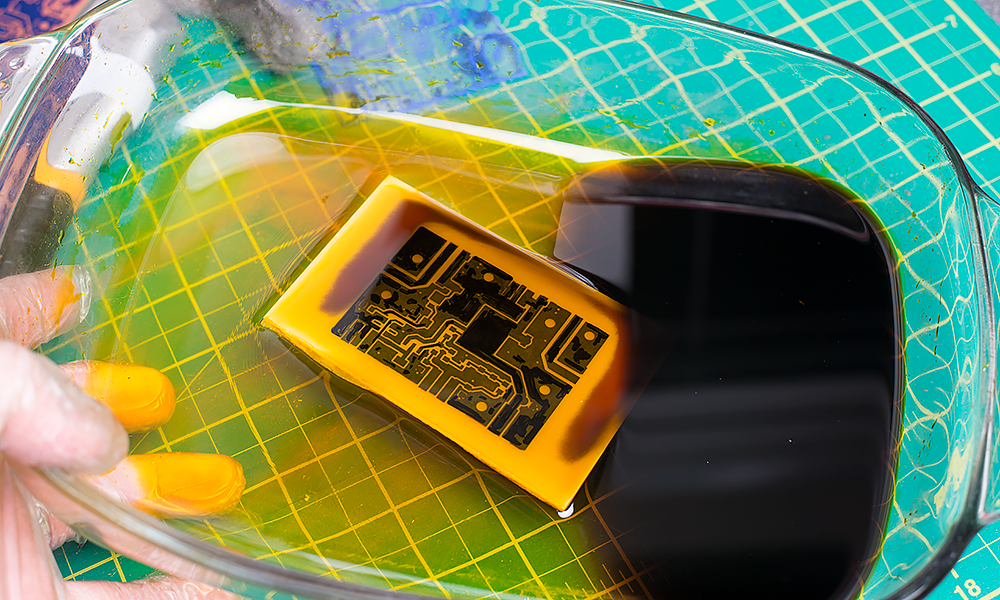
Before proceeding with the next step I relocated to my well ventilated garage and donned some rubber gloves and protective goggles. I poured a small amount of ferric chloride into a glass Pyrex dish and placed my PCB in the etching solution . I gently moved the Pyrex dish backwards and forwards to cover the board in solution. I did this every ten minutes or so for around 40 minutes to ensure fresh solution was cycled over the board. After all copper was removed from the PCB I used tweezers to remove the PCB from the solution. After wiping away excess etching solution with cloth I then washed it in fresh water. The etching solution was still good so I poured the used solution into a glass jar for future use.
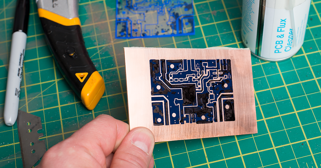
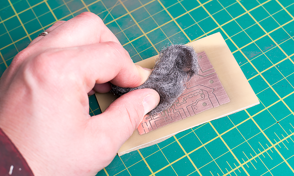
REMOVING FILM AND CLEANING THE PCB
After drying the PCB I removed the film using steel wool. After all of the film was removed I moved the wire wool along the length of the PCB in horizontal lines to key the copper in one direction. I then cleaned the tracks with PCB and flux cleaner.
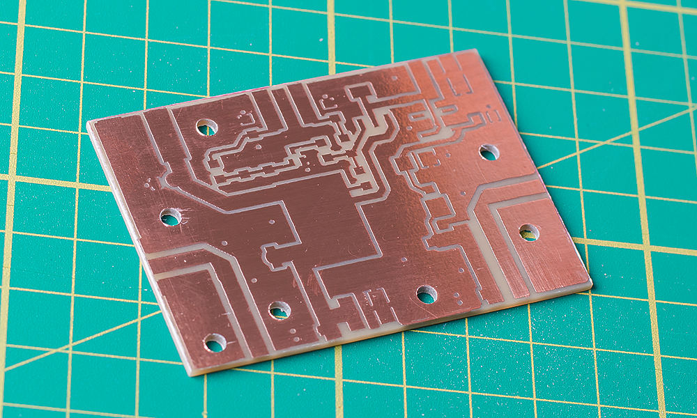
TRIMMING & FINISHING THE PCB
You will notice in the photo above that there was some excess board around the tracks. Before proceeding to the build stage I removed this excess using a technique that I will document in a separate article.
PROCESS COMPLETE
The process is now complete. The picture below shows the PCB complete with holes I drilled using a pillar drill. I made YouTube video below that incorporates all of the steps in this article – view it here.
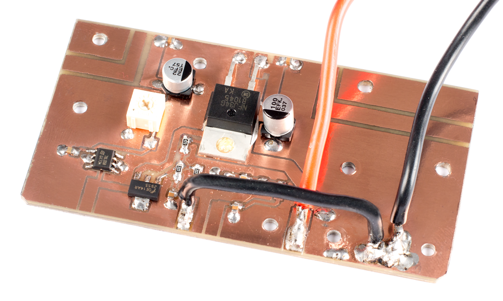
23CM LIQUID COOLED RF AMPLIFIER PROJECT
If you are interested in seeing how I used this technique for my 23cm liquid cooled RF amplifier project for ATV (Amateur Television) please click here.
Why not take a look at my YouTube channel here or Twitter posts here.
You can also register for my website here.
Thanks
73 de M0NWK
![]()